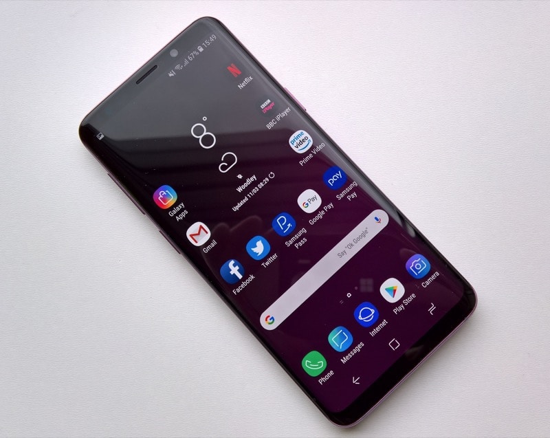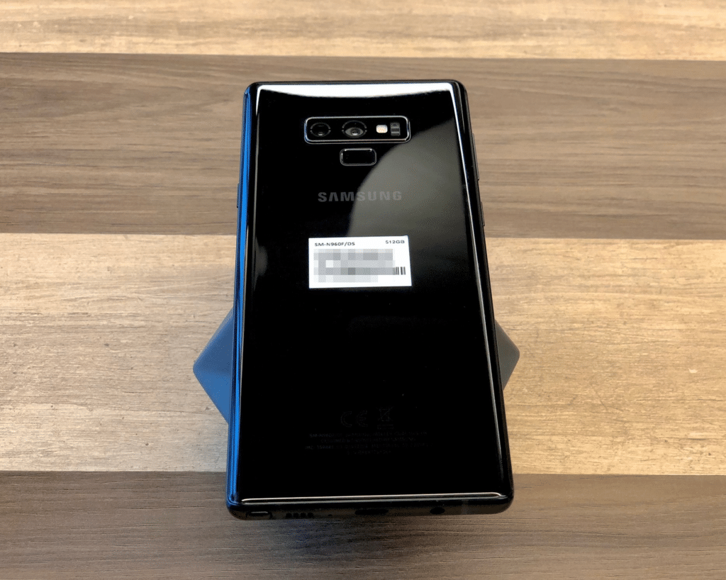
With the Galaxy Note 9 now on sale, the iFixit team has gone ahead and posted a detailed teardown of the handset. The teardown makes it pretty clear that accessing the internals of the Note 9 is as tough as its predecessor, the Note 8.
Getting inside the Note 9 requires prying open the back panel which has been tightly glued with the chassis. The very first thing to greet one once the backplate is out is the massive 4,000mAh battery which has also been glued to its place.
To accommodate for the bigger battery, Samsung has made the motherboard on the Note 9 bigger as it now also accommodates the daughterboard that was previously found on the Note 8. The USB-C port is modular in nature so that it can be easily replaced in case it ever goes kaput. The teardown also gives a clear glimpse at the beefy heat pipes the Note 9 comes with, though it fails to make any significant impact.

As for S Pen, it now features a lot of stuff inside despite its small size. There’s a Dialog Semiconductor Bluetooth Smart SoC and a Seiko supercapacitor which is good enough to power the S-Pen around 200-300 clicks.

Compared to the Note 8, Samsung has only made a few internal changes here and there to make room for the larger battery. In the process, Samsung has also made a lot of components inside the Note 9 modular in nature. None of the changes, however, help make it easier to repair the phone though. This is because gaining access to the internals of the phone requires one to pry open the rear glass which is stuck to the chassis using a copious amount of glue.
In the end, iFixit gives the Note 9 a repairability score of 4 out of 10 which essentially means repairing the device is going to be a nightmare of its own.
[Via iFixit]


